Simple Gate - not Sync design as it dont have registers
Notes
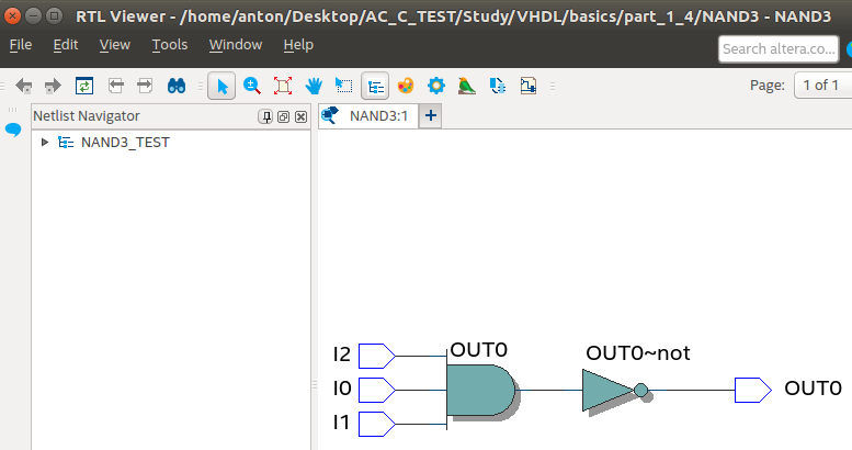
1. we cannot use a nand b nand c as nand is not associative logic operation.
2. to implement nand with 3 gates we can do it simple with and,not gates. like this : not(a and b and c).
3. nand gates are generic aka you can implement any other logic gate with several nand gates. (for xor we need 4 nand gates) this might be usefill when used old circuits that used TTL devices, as we may preffer 1 type of IC and use all its gate then solder several types when most if then not in use.
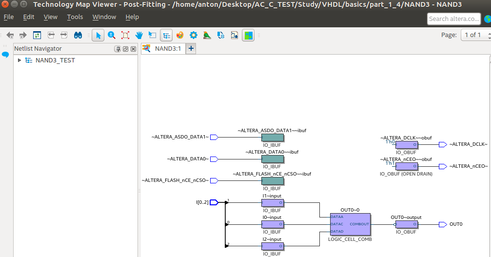
4. in modern FGPA there is no restriction or concern about logic elements quantity , anyway it preffer not to make complex code as it will make hard it to maintain, thus synthesis S\W will transte and optimize it on her own.
it mean that not(a and b and c) style are preffered!

we used TCL basec script to simulate the logic. note that we didnt use "add wave *" but added every signal\port one by one, using add wave nameOfSignal\port, also we added seperator to the waveform , it can be usefill when design contain a very large amount of signals.
Example of TCL Script


below are wave form that represend behaive of the NAND3 Gate, we used add wave -divide "internal" to represend the internal signals more clearly, in large systems number of signals will be inclresed significatnly and arranging waveform tools can be usefull.
only when all inputs are '1' the output will be '0', we didnt conver all the permutations as it not nessesary. also to do this (cover all testing permutations) it preffer to use Test Bench that can use loops or a Automatically generated Test Patterns.